SiO2/Al2O3/HfO2 Selective Buried Oxide Layer (SELBOX) Engineering and Its Influence on 20 nm n-MOSFET
DOI:
https://doi.org/10.51173/eetj.v3i1.29Keywords:
Al2O3, HfO2, n-MOSFET, SELBOX, Silvaco ATLAS, Breakdown voltageAbstract
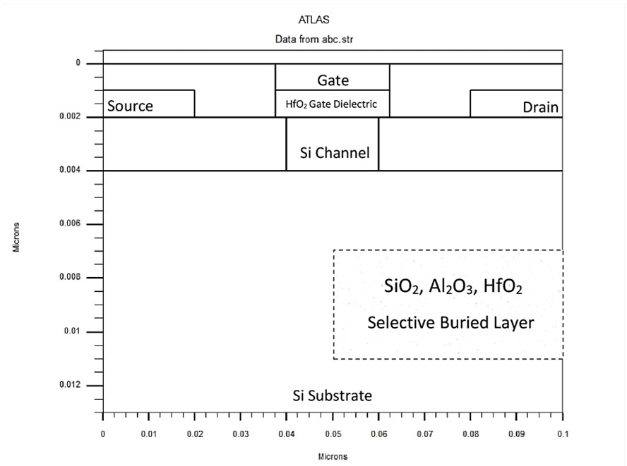
Short channel effects (SCEs) of nano-scaled n-MOSFET are solved by various techniques, one of which is the Selective buried oxide layer (SELBOX), which is implanted in the substrate of the MOSFET. This work involves simulating a 20 nm n-MOSFET with HfO2 gate dielectric using TCAD Silvaco ATLAS, and adding a SELBOX beneath the drain area at 30 nm depth. The scenario of this work is using three materials, SiO2, Al2O3, and HfO2, separately as a SELBOX. Also, the performance of the device is examined by shifting the SELBOX from 30 nm depth to direct contact with the channel position. The results depend on the band gap value of the material and its closeness to the drain region, which influences MOSFET performance. So, the comparison of the results will be between the standard design of MOSFET (without a SELBOX) and the design with the SELBOX, which has direct contact position with the channel. For SiO2 SELBOX material, the leakage current is decreased by 33% and breakdown voltage is increased from 85.09 V to 491.4 V. Al2O3 SELBOX material, the leakage current is decreased by 27%, and breakdown voltage is increased from 85.09 V to 275.7 V. Finally, for HfO2SELBOX, the leakage current is increased by 21%, and breakdown voltage is increased from 85.09 V to 172.3 V.
References
M. Aditya, K. S. Rao, B. Balaji, and K. G. Sravani, "Comparison of drain current characteristics of advanced MOSFET structures-a review," Silicon, vol. 14, no. 14, pp. 8269-8276, 2022. https://doi.org/10.1007/s12633-021-01638-8
R. H. Ahmed and A. S. Nouri, "Enhanced Transient Stability in Power Systems via Intelligent Control of SVCs Using Neural Networks," Electrical Engineering Technical Journal, vol. 2, no. 2, pp. 17-24, 2025. https://doi.org/10.51173/eetj.v2i2.23
S. M. Ferhan and H. Agahi, "Multi-Objective Optimization of Hybrid Energy Systems," Electrical Engineering Technical Journal, vol. 2, no. 2, pp. 1-16, 2025. https://doi.org/10.51173/eetj.v2i2.22
K. Pradhan, P. Agarwal, P. Sahu, and S. Mohapatra, "Role of high-k materials in Nanoscale TM-DG MOSFET: A simulation study," Invertis Journal of Science & Technology, vol. 6, no. 4, pp. 195-199, 2013.
B. Majkusiak, T. Janik, and J. Walczak, "Semiconductor thickness effects in the double-gate SOI MOSFET," IEEE Transactions on Electron Devices, vol. 45, no. 5, pp. 1127-1134, 2002. https://doi.org/10.1109/16.669563
H. Yu et al., "Energy gap and band alignment for (HfO 2) x (Al 2 O 3) 1− x on (100) Si," Applied Physics Letters, vol. 81, no. 2, pp. 376-378, 2002. https://doi.org/10.1063/1.1492024
M. Narayanan, H. Al-Nashash, B. Mazhari, D. Pal, and M. Chandra, "Analysis of kink reduction in SOI MOSFET using selective back oxide structure," Active and Passive Electronic Components, vol. 2012, no. 1, p. 565827, 2012. https://doi.org/10.1155/2012/565827
B. Thakral, G. Bakshi, and A. K. Kushwaha, "A review on SOI MOSFET and kink reduction using selective back oxide structure," in 2014 International Conference on Reliability Optimization and Information Technology (ICROIT), 2014: IEEE, pp. 487-490. https://doi.org/10.1109/ICROIT.2014.6798372
M. Narayanan and H. Al Nashash, "Minimization of self-heating in SOI MOSFET devices with SELBOX structure," in 2016 11th International Conference on Advanced Semiconductor Devices & Microsystems (ASDAM), 2016: IEEE, pp. 61 https://doi.org/10.1109/ASDAM.2016.7805895
R. Mahmoud, N. Madathumpadical, and H. Al-Nashash, "TCAD simulation and analysis of selective buried oxide MOSFET dynamic power," Journal of Low Power Electronics and Applications, vol. 9, no. 4, p. 29, 2019. https://doi.org/10.3390/jlpea9040029
S. Yoo and S. Kim, "Leakage optimization of the buried oxide substrate of nanosheet field-effect transistors," IEEE Transactions on Electron Devices, vol. 69, no. 8, pp. 4109-4114, 2022. https://doi.org/10.1109/TED.2022.3182300
M. Murshid and F. Bashir, "Ground plane and selective buried oxide based planar junctionless transistor," Frequenz, vol. 76, no. 1-2, pp. 1-7, 2022. https://doi.org/10.1515/freq-2021-0059
V. P. Tayade and S. L. Lahudkar, "Implementation of 20 nm graphene channel field effect transistors using silvaco TCAD tool to improve short channel effects over conventional MOSFETs," Advances in Technology Innovation, vol. 7, no. 1, pp. 18-29, 2021. https://doi.org/10.46604/aiti.2021.8098
J.-T. Park and J.-P. Colinge, "Multiple-gate SOI MOSFETs: device design guidelines," IEEE transactions on electron devices, vol. 49, no. 12, pp. 2222-2229, 2002. https://doi.org/10.1109/TED.2002.805634
T. Ernst, R. Ritzenthaler, O. Faynot, and S. Cristoloveanu, "A model of fringing fields in short-channel planar and triple-gate SOI MOSFETs," IEEE transactions on electron devices, vol. 54, no. 6, pp. 1366-1375, 2007. https://doi.org/10.1109/TED.2007.895241
A. Aminbeidokhti, A. A. Orouji, S. Rahmaninezhad, and M. Ghasemian, "A novel high-breakdown-voltage SOI MESFET by modified charge distribution," IEEE transactions on electron devices, vol. 59, no. 5, pp. 1255-1262, 2012. https://doi.org/10.1109/TED.2012.2186580
D. Madadi, A. A. Orouji, and A. Abbasi, "Improvement of nanoscale SOI MOSFET heating effects by vertical Gaussian drain-source doping region," Silicon, vol. 13, no. 3, pp. 645-651, 2021. https://doi.org/10.1007/s12633-020-00453-x
M. G. C. de Andrade and J. A. Martino, "Threshold voltages of SOI MuGFETs," Solid-State Electronics, vol. 52, no. 12, pp. 1877-1883, 2008. https://doi.org/10.1016/j.sse.2008.06.046
Downloads
Published
How to Cite
Issue
Section